1>> Explain basic computer organization and enlist various design components.
ANS---->. Computer organization refers to the way in which a computer's various components work together to execute instructions and perform tasks. The basic computer organization includes various design components, which are as follows:
Central Processing Unit (CPU): It is the brain of the computer that performs all the arithmetic and logical operations. The CPU consists of an arithmetic logic unit (ALU) that performs arithmetic and logical operations, a control unit (CU) that fetches instructions from memory and decodes them, and registers that store data.
Memory Unit: It is the component of the computer that stores instructions and data. The memory unit consists of two types of memory: primary memory and secondary memory. Primary memory, also known as main memory, includes Random Access Memory (RAM) and Read-Only Memory (ROM), while secondary memory includes hard disks, floppy disks, and optical disks.
Input Devices: These are the devices that allow the computer to accept data and instructions from the user. Examples of input devices include keyboards, mice, scanners, and microphones.
Output Devices: These are the devices that allow the computer to present data and information to the user. Examples of output devices include monitors, printers, and speakers.
System Bus: It is the communication channel that allows data to be transferred between the CPU, memory, and input/output devices.
Control Unit: It is the component of the CPU that manages the flow of data and instructions within the computer.
Arithmetic Logic Unit (ALU): It is the component of the CPU that performs arithmetic and logical operations on data.
Registers: They are small, high-speed memory locations within the CPU that store data and instructions temporarily.
Cache Memory: It is a small, high-speed memory location within the CPU that stores frequently used instructions and data.
Secondary Storage Devices: They are the devices that store data and programs for long-term use. Examples of secondary storage devices include hard disks, floppy disks, and optical disks.
Overall, these design components work together to form the basic computer organization and enable the computer to execute instructions and perform tasks.
2>> Draw & explain memory hierarchy in detail.
ANS----> Memory hierarchy refers to the organization of different types of storage devices that a computer system uses to store and retrieve data. The hierarchy is designed in such a way that the data can be accessed in the most efficient manner possible. The memory hierarchy typically includes several levels of storage devices, each with different characteristics such as speed, capacity, and cost.
Here is a diagram of the memory hierarchy:
CPU Registers -> Cache Memory -> Main Memory (RAM) -->Secondary-->Storage--> Devices-->Tertiary Storage Devices
Let's explore each level in detail:
CPU Registers: Registers are the fastest and smallest type of memory, located within the CPU itself. Registers are used to store data that is frequently accessed by the CPU, such as variables, addresses, and intermediate results during processing.
Cache Memory: Cache memory is a small and fast memory that sits between the CPU and main memory (RAM). The cache is designed to store frequently accessed data from main memory to reduce the time it takes to access that data. There are different levels of cache, with L1 cache being the fastest and smallest, and L3 cache being the largest and slowest.
Main Memory (RAM): RAM is the main memory of a computer system, used to temporarily store data and instructions that the CPU needs to access quickly. Main memory is faster than secondary and tertiary storage, but slower than CPU registers and cache memory. RAM is volatile, which means that its contents are lost when power is turned off.
Secondary Storage Devices: Secondary storage devices are non-volatile storage devices used for long-term storage of data and programs. Examples of secondary storage devices include hard disk drives (HDDs), solid-state drives (SSDs), optical disks, and magnetic tapes. Secondary storage devices are slower than main memory but offer much larger storage capacity.
Tertiary Storage Devices: Tertiary storage devices are used for archival and backup purposes. Examples of tertiary storage devices include tape libraries and optical jukeboxes. These devices offer very large storage capacity but are much slower than secondary storage devices.
In summary, the memory hierarchy is designed to optimize data access speed, storage capacity, and cost by using different types of storage devices at different levels. The higher up the hierarchy, the faster and more expensive the storage devices become. The lower down the hierarchy, the slower and cheaper the storage devices become.
3>> Explain in brief following terms: (i)Main memory & (ii) Cache memory
ANS----> (i) Main memory: Main memory, also known as Random Access Memory (RAM), is the primary memory of a computer system where the data and instructions that are currently being used by the CPU are stored temporarily. Main memory is volatile, which means that its contents are lost when power is turned off. RAM is much faster than secondary and tertiary storage devices, such as hard disk drives and optical disks, but slower than CPU registers and cache memory. The size of the main memory determines how much data and instructions the CPU can access at a given time.
(ii) Cache memory: Cache memory is a small, fast memory that is located between the CPU and main memory. The cache is designed to store frequently accessed data from main memory to reduce the time it takes to access that data. Cache memory is much faster than main memory, and its small size allows it to be accessed much more quickly. There are different levels of cache, with L1 cache being the fastest and smallest, and L3 cache being the largest and slowest. The cache uses a hierarchy to determine which data to store and how long to store it, based on the frequency of access and the size of the cache. By using cache memory, the CPU can access frequently used data much more quickly, improving overall system performance.
4>> alculate execution time of program for following given data: > Total instruction count = 10000 instructions
> CPI (Cycles/Instructions) = 2.5 cycles/instructions
> CPU clock rate = 5 MHz
ANS---->. We can use the following formula to calculate the execution time of a program:
Execution time (in seconds) = (Total instruction count) x CPI / CPU clock rate
Given data:
Total instruction count = 10000 instructions CPI = 2.5 cycles/instruction CPU clock rate = 5 MHz
Substituting the values in the formula, we get:
Execution time = (10000 instructions) x (2.5 cycles/instruction) / (5 MHz) Execution time = (25000 cycles) / (5,000,000 cycles/second) Execution time = 0.005 seconds
Therefore, the execution time of the program is 0.005 seconds or 5 milliseconds.
5>>. Explain difference between RISC & CISC.
ANS----> RISC (Reduced Instruction Set Computing) and CISC (Complex Instruction Set Computing) are two different approaches to computer processor design.
RISC processors use a simplified instruction set that performs simple operations in a single clock cycle. RISC processors have a small and fast cache memory, which is used to store frequently used instructions and data. RISC processors typically have a larger number of registers, which are used to store data and intermediate results during processing. The RISC design philosophy emphasizes simplicity, efficiency, and a large number of simple instructions.
CISC processors, on the other hand, use a more complex instruction set that performs multiple operations in a single instruction. CISC processors have a larger and slower cache memory, which is used to store both instructions and data. CISC processors typically have a smaller number of registers, and use memory more frequently for data storage. The CISC design philosophy emphasizes ease of use and a smaller number of complex instructions.
Overall, the key difference between RISC and CISC is in the complexity of the instruction set. RISC processors use a simpler and more streamlined instruction set, while CISC processors use a more complex and feature-rich instruction set. RISC processors are generally faster and more efficient, while CISC processors are generally more versatile and easier to use.
6>>. Explain Flynn's classification(taxonomy) of computers
ANS----> Flynn's classification, also known as Flynn's taxonomy, is a way of categorizing computer architectures based on the number of instruction streams and data streams that are processed concurrently. The classification was proposed by Michael J. Flynn in 1966 and is widely used in computer science.
There are four categories in Flynn's taxonomy:
SISD (Single Instruction Single Data): SISD is the simplest type of computer architecture, in which a single instruction stream operates on a single data stream. This is the traditional Von Neumann architecture, where a single processor sequentially executes instructions from memory on a single data item at a time.
7>>. What is parallel processing and explain its significance.
ANS----> Parallel processing is a computing paradigm in which multiple processors or processor cores work together to perform a single task. Parallel processing can be used to speed up computations and increase the processing power of a computer system.
In a parallel processing system, the workload is divided into smaller sub-tasks, and each sub-task is assigned to a different processor or processor core. The processors work simultaneously to complete their respective sub-tasks, and the results are combined to produce the final output.
Parallel processing has several significant advantages:
Speedup: Parallel processing can significantly reduce the time it takes to complete a task. By dividing the workload among multiple processors, each processor can work on a smaller portion of the task, and the task can be completed much faster than with a single processor.
Scalability: Parallel processing can be scaled up or down depending on the size and complexity of the task. As the workload increases, more processors can be added to the system to handle the additional load.
Cost-effective: Parallel processing can be a cost-effective solution for processing large amounts of data or complex calculations. By using multiple inexpensive processors instead of a single expensive processor, the cost of the system can be reduced.
Fault tolerance: Parallel processing systems can be designed to be fault-tolerant. If one processor fails, the other processors can continue to work on the task, ensuring that the system remains operational.
Parallel processing is used in a wide range of applications, including scientific simulations, weather forecasting, financial modeling, and image and video processing. With the increasing availability of multi-core processors and distributed computing systems, parallel processing has become an essential tool for improving the performance and scalability of modern computing systems.
8>> Define pipelining and explain it with appropriate example
ANS-->Pipelining is a technique used in computer architecture to increase the throughput of a processor by dividing the instruction processing into stages. In pipelining, multiple instructions are executed simultaneously, with each instruction passing through a series of stages, where each stage performs a specific operation.
For example, let's consider the following instruction sequence:
ADD R1, R2, R3 SUB R4, R5, R6 MUL R7, R8, R9 DIV R10, R11, R12
In a non-pipelined architecture, each instruction must complete its execution before the next instruction can be executed. This can result in idle time for the processor between instructions, reducing the overall throughput.
In a pipelined architecture, the instruction processing is divided into stages, and multiple instructions can be in different stages of processing at the same time. For example, let's say our processor has four stages: instruction fetch (IF), instruction decode (ID), execute (EX), and writeback (WB).
In a pipelined architecture, the four instructions above would be processed in the following manner:
Cycle 1: Instruction 1 is fetched and enters the IF stage. Cycle 2: Instruction 1 moves to the ID stage, and Instruction 2 enters the IF stage. Cycle 3: Instruction 1 moves to the EX stage, Instruction 2 moves to the ID stage, and Instruction 3 enters the IF stage. Cycle 4: Instruction 1 moves to the WB stage, Instruction 2 moves to the EX stage, Instruction 3 moves to the ID stage, and Instruction 4 enters the IF stage. Cycle 5: Instruction 2 moves to the WB stage, Instruction 3 moves to the EX stage, and Instruction 4 moves to the ID stage. Cycle 6: Instruction 3 moves to the WB stage, and Instruction 4 moves to the EX stage. Cycle 7: Instruction 4 moves to the WB stage.
In this example, each instruction is divided into four stages, and the stages are overlapped to allow multiple instructions to be in different stages simultaneously. This increases the throughput of the processor and reduces the idle time between instructions.
Overall, pipelining is a powerful technique that allows for the processing of multiple instructions simultaneously, improving the performance and throughput of the processor.
9>> Explain instruction pipelining in detail
ANS--->Instruction pipelining is a technique used in computer architecture to increase the processing speed of a processor. It involves breaking down the execution of an instruction into multiple stages and processing multiple instructions simultaneously, with each instruction passing through a series of stages.
The stages in an instruction pipeline typically include:
Instruction Fetch (IF): The instruction is fetched from memory and loaded into the instruction register.
Instruction Decode (ID): The instruction is decoded to determine what operation needs to be performed and what operands are required.
Execution (EX): The operation is performed, and the result is stored in a register.
Memory Access (MEM): If the instruction involves accessing memory, the memory is accessed to load or store data.
Write-Back (WB): The result of the operation is written back to memory or to a register.
The idea behind instruction pipelining is that each stage can be performed independently and simultaneously on multiple instructions, allowing for higher throughput and faster execution of instructions.
For example, let's consider the following sequence of instructions:
ADD R1, R2, R3 SUB R4, R5, R6 MUL R7, R8, R9 DIV R10, R11, R12
In a non-pipelined architecture, the processor would execute one instruction at a time, waiting for each instruction to complete before starting the next one. This would result in a longer execution time, as there would be idle time between instructions.
In a pipelined architecture, the execution of instructions is overlapped, and multiple instructions are in different stages of execution at the same time. For example, while the ADD instruction is being executed in the EX stage, the SUB instruction can be fetched in the IF stage, and the MUL instruction can be decoded in the ID stage.
However, there are certain challenges associated with instruction pipelining, including data hazards and control hazards. Data hazards occur when an instruction requires data that is not yet available, while control hazards occur when the next instruction cannot be determined until the current instruction has completed.
To overcome these challenges, various techniques such as forwarding and branch prediction are used in modern pipelined architectures.
Overall, instruction pipelining is a powerful technique that allows for faster execution of instructions by breaking them down into multiple stages and processing them simultaneously. By overlapping the execution of multiple instructions, pipelining improves the performance and throughput of modern processors.
10>>What are Array processors and also explain in brief
ANS-- An array processor is a type of parallel processing system that is designed to perform operations on arrays or matrices of data. It consists of a large number of processing elements that are arranged in an array-like structure, and each processing element can perform a specific operation on a subset of the data. This allows for the processing of large amounts of data in parallel, which can significantly increase performance.
There are two main types of array processors: attached array processors and SIMD array processors.
(i) Attached Array Processors: In this type of array processor, the processing elements are physically attached to the main processor, and they share the same memory. The main processor controls the operation of the attached array processor and can transfer data to and from it as needed. Attached array processors are typically used for scientific and engineering applications that require large amounts of number-crunching.
(ii) SIMD Array Processors: In this type of array processor, the processing elements are connected in a single instruction, multiple data (SIMD) architecture, which means that each processing element performs the same operation on different elements of the data in parallel. SIMD array processors are used for applications such as image and video processing, where the same operation needs to be performed on a large number of pixels or frames in parallel.
SIMD array processors can be further classified into two types: static SIMD array processors and dynamic SIMD array processors. Static SIMD array processors have a fixed number of processing elements that are organized into a fixed number of SIMD lanes, whereas dynamic SIMD array processors can dynamically allocate processing elements to different SIMD lanes based on the workload.
Overall, array processors are useful for applications that require large amounts of parallel processing, such as scientific simulations, image and video processing, and machine learning.
11>>What are Multiprocessors & discuss the characteristics of a Multiprocessors ?
ANS---->Multiprocessors are computer systems that use multiple processors to execute tasks. These systems can range from a small number of processors in a single machine to thousands of processors in a distributed system. Multiprocessors can be classified into two categories: Shared Memory Multiprocessors and Distributed Memory Multiprocessors.
Shared Memory Multiprocessors: In a shared memory multiprocessor, all processors have access to a single shared memory. The processors communicate with each other by reading and writing to shared memory. The key characteristics of a shared memory multiprocessor are:
Scalability: The number of processors can be increased or decreased to match the processing needs of the system.
High Performance: Shared memory access is faster than communication across different processors, so shared memory multiprocessors can provide high performance.
Memory Consistency: All processors see the same view of shared memory at any given time. This requires special mechanisms to ensure that the shared memory is always in a consistent state.
Cache Coherence: Since each processor has its own cache, cache coherence protocols are used to ensure that all processors see the same value in shared memory.
Distributed Memory Multiprocessors: In a distributed memory multiprocessor, each processor has its own private memory and communicates with other processors by passing messages over a network. The key characteristics of a distributed memory multiprocessor are:
High Scalability: Distributed memory multiprocessors can be scaled to thousands of processors by adding more nodes to the network.
Low Latency: Message passing over a local network can be very fast, resulting in low latency communication.
Parallelism: Since each processor has its own memory, they can execute tasks independently, resulting in high parallelism.
No Memory Consistency: Each processor has its own memory, so there is no global consistency model. This requires careful programming to avoid race conditions and other concurrency issues.
Overall, multiprocessors provide high performance and scalability, making them ideal for tasks that require a lot of processing power. However, they also require careful programming and management to ensure that they operate efficiently and effectively.
12>> Enlist types of Interconnection structure in Multiprocessors & explain any one in detail.
ANS--> There are several types of interconnection structures used in multiprocessors, each with its own advantages and disadvantages. Some of the common types of interconnection structures are:
Shared Bus: A shared bus interconnects all processors and memory through a single bus, allowing each processor to access the memory and other processors by arbitrating access to the bus. This is a simple and low-cost interconnect structure, but it can become a bottleneck when the number of processors increases.
Crossbar Switch: A crossbar switch interconnects processors and memory through a network of switches that provide a direct connection between any pair of processors and memory. This is a scalable and high-performance interconnect structure, but it is expensive to implement.
Mesh Network: In a mesh network, each processor is connected to its neighboring processors through a direct link, forming a grid-like structure. This is a highly scalable interconnect structure, but it can become complex to manage as the number of processors increases.
Hypercube: A hypercube interconnects processors and memory through a network of switches that form a multidimensional cube-like structure. This is a highly scalable and fault-tolerant interconnect structure, but it can be expensive to implement.
One example of an interconnection structure is a crossbar switch, which is commonly used in large-scale multiprocessors. In a crossbar switch, processors and memory are connected through a network of switches that provide a direct connection between any pair of processors and memory. Each switch is controlled by an arbitration mechanism that determines which processor or memory module can access the switch at any given time
The key advantage of a crossbar switch is its high performance and scalability. Because each processor and memory module has a direct connection to every other processor and memory module, there are no bottlenecks or contention for shared resources. This allows for high-speed communication and efficient use of resources, making crossbar switches ideal for large-scale multiprocessors.
However, crossbar switches can also be expensive to implement, as they require a large number of switches and interconnects. Additionally, they can be difficult to manage, as the arbitration mechanisms and routing algorithms can be complex to implement and optimize.
13>> Explain interconnection structure in Multiprocessors in detail.
ANS---->In a multiprocessor system, the interconnection structure is the network of communication pathways that connect the processors, memory, and input/output devices. The interconnection structure plays a crucial role in determining the performance and scalability of the multiprocessor system.
There are several types of interconnection structures used in multiprocessors, each with its own advantages and disadvantages. Some of the common types of interconnection structures are:
Shared Bus: A shared bus interconnects all processors and memory through a single bus, allowing each processor to access the memory and other processors by arbitrating access to the bus. This is a simple and low-cost interconnect structure, but it can become a bottleneck when the number of processors increases.
Crossbar Switch: A crossbar switch interconnects processors and memory through a network of switches that provide a direct connection between any pair of processors and memory. This is a scalable and high-performance interconnect structure, but it is expensive to implement.
Mesh Network: In a mesh network, each processor is connected to its neighboring processors through a direct link, forming a grid-like structure. This is a highly scalable interconnect structure, but it can become complex to manage as the number of processors increases.
Hypercube: A hypercube interconnects processors and memory through a network of switches that form a multidimensional cube-like structure. This is a highly scalable and fault-tolerant interconnect structure, but it can be expensive to implement
In a crossbar switch interconnect, each processor and memory module has a direct connection to every other processor and memory module through a network of switches. The switches are controlled by an arbitration mechanism that determines which processor or memory module has access to each switch at any given time. This type of interconnect is highly scalable and provides high performance, but it can be expensive to implement.
In a mesh network interconnect, each processor is connected to its neighboring processors through a direct link, forming a grid-like structure. This type of interconnect is highly scalable, but it can become complex to manage as the number of processors increases.
In a hypercube interconnect, processors and memory modules are connected through a multidimensional cube-like network of switches. This type of interconnect is highly scalable and fault-tolerant, but it can be expensive to implement.
The choice of interconnect structure depends on the requirements of the multiprocessor system, such as the number of processors, the communication bandwidth needed, the cost of the system, and the ease of management. In general, high-performance systems require high-bandwidth interconnects, while cost-effective systems require low-cost interconnects.
14>>What is Interprocessor arbitration & explain series and parallel arbitration in brief ?
ANS---->Interprocessor arbitration is the process by which multiple processors in a multiprocessor system compete for access to shared resources, such as memory or input/output devices. The arbitration mechanism is responsible for resolving conflicts between processors and ensuring that only one processor at a time can access a shared resource.
There are two main types of interprocessor arbitration: series arbitration and parallel arbitration.
In series arbitration, each processor is connected to a common arbiter that determines which processor has access to a shared resource. When a processor wants to access the shared resource, it sends a request to the arbiter. The arbiter then evaluates the requests from all processors and selects one to grant access to the shared resource. The selected processor can then access the resource while the other processors wait for their turn.
Series arbitration is simple to implement, but it can lead to performance degradation as only one processor can access the shared resource at a time, which can result in increased latency and decreased throughput.
In parallel arbitration, each processor has a dedicated path to the shared resource and can request access to it directly. When multiple processors request access simultaneously, the arbitration mechanism resolves the conflict and grants access to one of the processors based on a predetermined priority or fairness criteria.
Parallel arbitration can improve system performance by allowing multiple processors to access the shared resource simultaneously, reducing latency and increasing throughput. However, it can be more complex to implement than series arbitration, as each processor needs a dedicated path to the shared resource.
The choice between series and parallel arbitration depends on the specific requirements of the multiprocessor system, such as the number of processors, the communication bandwidth needed, and the complexity of the arbitration mechanism.
15>>Write a short note on shared memory multiprocessors
ANS-->>In a shared memory multiprocessor system, all processors share a common physical memory, allowing any processor to access any location in memory. This type of multiprocessor system is also known as a Symmetric Multiprocessor (SMP) system.
In a shared memory system, multiple processors can work on the same data simultaneously, increasing the overall system performance. The processors communicate with each other by reading and writing to the shared memory, which provides a fast and efficient means of interprocessor communication.
Shared memory multiprocessors are commonly used in applications that require high performance, such as scientific simulations, data analysis, and large-scale databases. They are also used in computer servers and high-end workstations that require processing power for demanding applications.
However, shared memory multiprocessors have some limitations. As the number of processors increases, the shared memory can become a bottleneck, leading to decreased performance. Additionally, shared memory systems require a mechanism for managing access to shared resources, such as semaphores or locks, to prevent data inconsistency and race conditions.
Overall, shared memory multiprocessors provide a fast and efficient means of interprocessor communication, but require careful design and management to ensure optimal performance and scalability.
16>> Draw neat & clean pin diagram of 8085 microprocessor.
ANS---->

17>>Draw and explain pin diagram of 8085 microprocessor.
ANS---->. The 8085 microprocessor has a total of 40 pins, which are divided into four functional groups: power supply and clock signals, address bus, data bus, and control and status signals.
- Power supply and clock signals: The first group of pins in the 8085 microprocessor consists of three pins: Vcc, GND, and CLK.
- Vcc is the power supply pin that is connected to a +5V DC power supply.
- GND is the ground pin that is connected to the ground of the circuit.
- CLK is the clock input pin that is used to provide the timing signal to the microprocessor. The clock frequency determines the speed of the microprocessor.
Address bus: The address bus consists of 16 pins (A0-A15) which are used to provide the memory address to the microprocessor. These pins are used to specify the location of the data or instruction to be read or written from/to the memory.
Data bus: The data bus consists of eight pins (D0-D7) which are used to transmit the data between the microprocessor and external devices. These pins are bidirectional and are used to transfer data in and out of the microprocessor.
Control and status signals: The control and status signals group consists of 18 pins (AD0-AD7, ALE, RD, WR, IO/M, S1, S0, and RESET) which are used to control the operation of the microprocessor and to indicate its status.
- AD0-AD7 pins are multiplexed address/data pins which are used to provide both address and data information to the microprocessor.
- ALE (Address Latch Enable) is a pulse signal that is used to latch the address from the address bus onto the address latch circuitry inside the microprocessor.
- RD (Read) and WR (Write) are control signals that are used to initiate a read or write operation on the data bus.
- IO/M (Input/Output and Memory) is a control signal that determines whether the microprocessor is accessing memory or I/O devices.
- S1 and S0 are status signals that are used to indicate the status of the microprocessor.
- RESET is a control signal that is used to reset the microprocessor to its initial state.
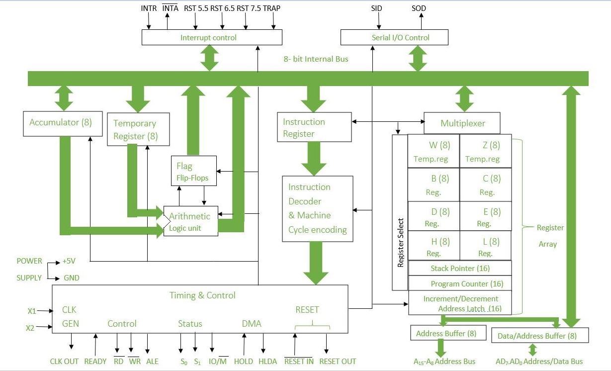
Arithmetic and Logic Unit (ALU): The ALU is responsible for performing arithmetic and logical operations on data. It consists of two 8-bit registers, the Accumulator (ACC) and the Temporary Register (TMP), as well as a set of flags that indicate the status of the ALU operations. The ALU can perform basic arithmetic operations such as addition, subtraction, and multiplication, as well as logical operations such as AND, OR, and XOR.
Control Unit (CU): The control unit is responsible for controlling the flow of data and instructions within the microprocessor. It fetches instructions from memory, decodes them, and executes them. It consists of a control logic circuit that generates the necessary control signals to carry out the instructions. The control unit also contains a program counter (PC) that keeps track of the address of the next instruction to be executed.
Registers: The 8085 microprocessor has several registers that are used to store data and control the operation of the microprocessor. These registers include:
- Accumulator (ACC): a general-purpose register used for arithmetic and logical operations.
- Temporary Register (TMP): a register used to hold intermediate results during ALU operations.
- Program Counter (PC): a 16-bit register that keeps track of the address of the next instruction to be executed.
- Stack Pointer (SP): a 16-bit register that points to the top of the stack.
- Flag Register (FLAGS): a register that stores the status of the ALU operations. The flags include the Sign flag, Zero flag, Auxiliary Carry flag, Parity flag, and Carry flag.
The 8085 microprocessor also has a memory interface that allows it to access external memory and I/O devices. It has a 16-bit address bus and an 8-bit data bus that are used to transfer data between the microprocessor and external devices.
In summary, the architecture of the 8085 microprocessor consists of an ALU for performing arithmetic and logical operations, a control unit for controlling the flow of data and instructions, and registers for storing data and controlling the microprocessor operation.
< THE DIAGRAM IS AS IT IS THE 18TH QUESTION>
20>>Explain Address, Data & Control buses in 8085 microproccessor.
ANS---->.
Address Bus: The address bus in the 8085 microprocessor is a group of 16 bi-directional pins that are used to transmit memory address information from the microprocessor to external memory or I/O devices. These pins are labeled as A0 to A15 and can address a maximum of 64 KB of memory. The microprocessor generates a 16-bit address on these pins to select the location in memory where the data or instruction is stored or to be written.
Data Bus: The data bus in the 8085 microprocessor is a group of eight bi-directional pins that are used to transfer data between the microprocessor and external memory or I/O devices. These pins are labeled as D0 to D7 and are bidirectional. They can be used to transfer data from the microprocessor to an external device or to receive data from an external device. The data bus is used to transfer both instructions and data, depending on the type of operation being performed by the microprocessor.
Control Bus: The control bus in the 8085 microprocessor is a group of various bi-directional pins that are used to control the operation of the microprocessor and communicate status information. The following are the main control signals used by the 8085 microprocessor:
- RD (Read) and WR (Write): These signals are used to indicate whether the microprocessor is reading from or writing to external memory or I/O devices.
- ALE (Address Latch Enable): This signal is used to indicate that the microprocessor has placed a valid address on the address bus.
- IO/M (Input/Output and Memory): This signal is used to indicate whether the microprocessor is accessing memory or I/O devices.
- RESET: This signal is used to reset the microprocessor to its initial state.
- HOLD: This signal is used to request the microprocessor to release the buses for another device to use them.
- HLDA (Hold Acknowledge): This signal is used by the microprocessor to acknowledge the HOLD signal and release the buses for another device to use them.
- INTA (Interrupt Acknowledge): This signal is used by the microprocessor to acknowledge the interrupt request from an external device.
In summary, the address bus in the 8085 microprocessor is used to transmit memory address information, the data bus is used to transfer data between the microprocessor and external devices, and the control bus is used to control the operation of the microprocessor and communicate status information.
21>>Explain Control bus in detail with table showing IO/M, RD & WR operation.
ANS---->are used to control the operation of the microprocessor and communicate status information. The following are the main control signals used by the 8085 microprocessor:
IO/M (Input/Output and Memory): The IO/M signal is used to indicate whether the microprocessor is accessing memory or I/O devices. When this signal is high (logic 1), the microprocessor is accessing an I/O device, and when it is low (logic 0), the microprocessor is accessing memory.
RD (Read): The RD signal is used to indicate that the microprocessor is reading data from an external memory or I/O device. When this signal goes low (logic 0), the external device is enabled to send data to the microprocessor through the data bus.
WR (Write): The WR signal is used to indicate that the microprocessor is writing data to an external memory or I/O device. When this signal goes low (logic 0), the data on the data bus is latched into the external device.
Here is a table showing the IO/M, RD, and WR operations:
| IO/M | RD | WR | Operation |
|---|---|---|---|
| 0 | 1 | 0 | Memory Read Operation |
| 0 | 0 | 1 | Memory Write Operation |
| 1 | 1 | 0 | I/O Read Operation |
| 1 | 0 | 1 | I/O Write Operation |
In a memory read operation, the microprocessor places the memory address on the address bus and asserts the RD signal low. The external memory device then sends the data stored at the address to the microprocessor through the data bus.
In a memory write operation, the microprocessor places the memory address and data to be written on the address and data buses, respectively, and asserts the WR signal low. The external memory device then latches the data into the memory location specified by the address.
In an I/O read operation, the microprocessor places the I/O address on the address bus and asserts the RD signal low. The external I/O device then sends the data stored at the address to the microprocessor through the data bus.
In an I/O write operation, the microprocessor places the I/O address and data to be written on the address and data buses, respectively, and asserts the WR signal low. The external I/O device then latches the data into the specified I/O location.
In summary, the control bus in the 8085 microprocessor is used to control the operation of the microprocessor and communicate status information. The IO/M, RD, and WR signals are used to perform memory and I/O read and write operations.
22>>Draw & explain Flag register in detail
ANS---->
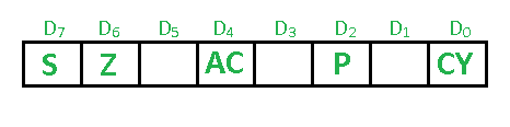
The flag register consists of five individual bits, which are used to indicate the status of different operations. The following table shows the five flag bits and their respective meanings:
| Flag Bit | Name | Description |
|---|---|---|
| D7 | Sign Flag | This bit is set if the result of an arithmetic or logic operation is negative. |
| D6 | Zero Flag | This bit is set if the result of an arithmetic or logic operation is zero. |
| D5 | Aux Carry Flag | This bit is set if there is a carry-out from bit 3 to bit 4 during an arithmetic operation. |
| D4 | Parity Flag | This bit is set if the result of an arithmetic or logic operation has an even number of set bits. |
| D3 | Carry Flag | This bit is set if there is a carry-out from the most significant bit during an arithmetic operation. |
The flag register is automatically updated by the microprocessor after an arithmetic or logic operation is performed. The status of the flag bits can be checked by a programmer to make decisions based on the outcome of the operation.
For example, the sign flag can be used to check whether the result of an operation is positive or negative, while the zero flag can be used to check if the result is zero. The carry flag is used to indicate if there is a carry-out from the most significant bit during an arithmetic operation, while the auxiliary carry flag is used to indicate if there is a carry-out from bit 3 to bit 4 during an arithmetic operation.
In summary, the flag register in the 8085 microprocessor is a special register that is used to indicate the status of certain arithmetic and logic operations. The five flag bits in the flag register are used to indicate whether the result of an operation is positive or negative, zero or non-zero, and whether there was a carry or an auxiliary carry during an arithmetic operation.
23>> Explain how de-multiplexing of AD0 - AD7 is done in 8085 microprocessor.
ANS---->The AD0-AD7 lines in the 8085 microprocessor are multiplexed with the lower 8 bits of the address bus (A0-A7). This means that during the first clock cycle of an instruction cycle, these lines are used as the lower 8 bits of the memory address, and during the second clock cycle, they are used as the data bus.
To separate the address and data signals, a demultiplexing circuit is used. This circuit uses a latch to store the address during the first clock cycle and then releases the address bus to be used for data during the second clock cycle.
The demultiplexing circuit consists of a latch (typically a D flip-flop) and an enable signal. The AD0-AD7 lines are connected to the input of the latch, and the output of the latch is connected to the lower 8 bits of the address bus (A0-A7).
During the first clock cycle, the enable signal is low, which causes the latch to store the value on the AD0-AD7 lines. At the end of the first clock cycle, the enable signal goes high, which disconnects the AD0-AD7 lines from the latch output and allows the address bus to use the stored value.
During the second clock cycle, the enable signal is again low, which allows the data to be placed on the AD0-AD7 lines. The data is then read from or written to the memory location specified by the address stored in the latch during the first clock cycle.
This demultiplexing process is used in the 8085 microprocessor to allow the same set of lines to be used for both address and data signals, reducing the number of pins required on the microprocessor and simplifying the circuitry needed to interface with the microprocessor.
24>>State the names of Control Signals in 8085 μP and how they are generated using IC 74LS138
ANS----> The 8085 microprocessor has several control signals that are used to synchronize and control its various operations. The following are the names of the control signals in the 8085 microprocessor:
- ALE (Address Latch Enable)
- RD (Read)
- WR (Write)
- IO/M (Input/Output or Memory Select)
- HLDA (Hold Acknowledge)
- READY (Ready)
These control signals are generated using various logic gates and circuits, including the IC 74LS138, which is a 3-to-8 decoder. The 74LS138 takes a 3-bit input (A15, IO/M, and RD/WR) and generates up to 8 output signals, depending on the input combination.
In the 8085 microprocessor, the A15 signal is used to indicate whether the current address being accessed is in the memory or I/O space. The IO/M signal is used to select either memory or I/O operations. The RD/WR signal is used to indicate whether the current operation is a read or write operation.
By connecting the A15, IO/M, and RD/WR signals to the input of the 74LS138, the decoder generates different combinations of output signals, which are then used to generate the control signals for the microprocessor.
For example, when the A15, IO/M, and RD/WR signals are 0, 1, and 0 respectively, the 74LS138 generates a low signal on its Y0 output. This output is connected to the ALE signal generator, which generates a pulse on the ALE line to latch the lower 8 bits of the address bus.
Similarly, when the A15, IO/M, and RD/WR signals are 1, 0, and 1 respectively, the 74LS138 generates a low signal on its Y3 output. This output is connected to the WR signal generator, which generates a write pulse to write the data on the data bus to the memory location specified by the address bus.
Therefore, the 74LS138 decoder plays a crucial role in generating the control signals required for the 8085 microprocessor to perform various operations.
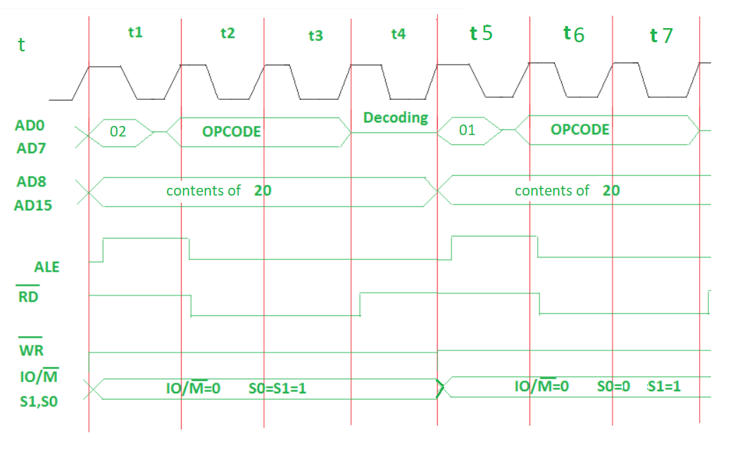
25>>Define (i) Instruction Cycle (ii) Machine Cycle & (iii) T-States
ANS---->In a microprocessor, the execution of an instruction involves a series of events that are timed by clock pulses. The following terms are used to describe these events:
Instruction Cycle: An instruction cycle is the time required for the execution of a single instruction. It consists of one or more machine cycles and is typically divided into fetch and execute phases.
Machine Cycle: A machine cycle is the basic operation of the microprocessor and is defined as the time required to complete one operation of the processor. It consists of several T-states, which are clock pulses used to synchronize the operation of the microprocessor.
T-States: T-states are the basic unit of timing in a microprocessor. They are short periods of time, typically a few nanoseconds, that are used to synchronize the operations of the microprocessor. Each T-state corresponds to one clock pulse, and the number of T-states required to execute an instruction varies depending on the complexity of the instruction.
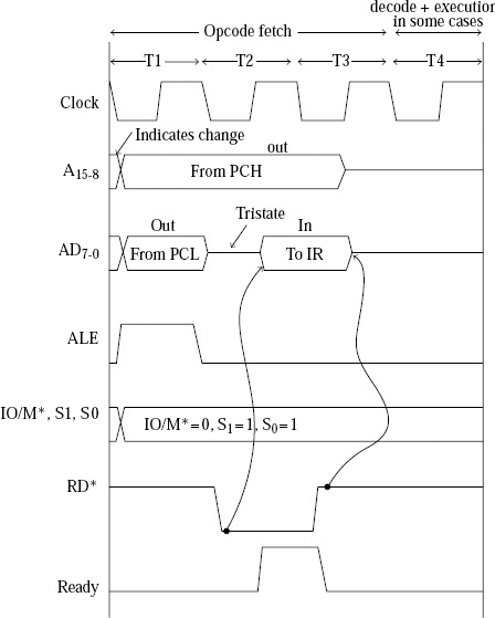

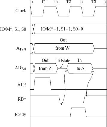
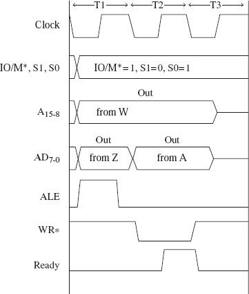
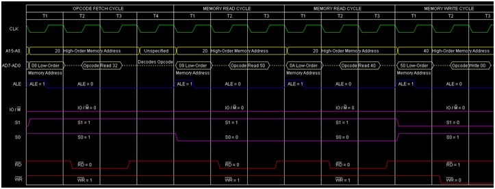
28>>Draw timing diagram of Memory Write machine cycle
ANS---->


34>>Draw timing diagram of instruction: INR B
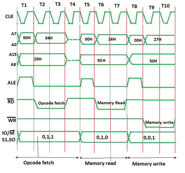
38>>Draw timing diagram of instruction: LDA 4040H
Assembly language and higher-level language are two different programming languages with distinct characteristics. Here are some differences between them:
Level of Abstraction: Assembly language is a low-level language that is specific to the hardware architecture. It is close to the machine language and provides direct access to the hardware resources. On the other hand, higher-level languages are abstract and independent of the hardware architecture. They use commands that are closer to natural language and are designed to be easily readable and writable by humans.
Complexity: Assembly language requires a great deal of knowledge and expertise about the hardware architecture. It is challenging to read, write and maintain assembly code, and the programs are typically longer than higher-level languages due to the need to specify each instruction. Higher-level languages are simpler and more natural to write and maintain, as they are designed to make programming tasks easier.
Portability: Assembly language programs are tied to the specific hardware architecture they are written for, making it difficult to port to other platforms. Higher-level languages, on the other hand, are more portable and can be used on multiple platforms with little modification.
Efficiency: Assembly language is more efficient than higher-level languages because it provides direct access to hardware resources. Higher-level languages, while more abstract, require more resources and translation to execute programs.
Development Time: Writing code in assembly language takes longer than writing in higher-level languages. The level of detail needed to write a functional assembly language program requires more time and attention to detail. Higher-level languages, on the other hand, allow for faster development, as they require less detail and are more intuitive.
Overall, Assembly language is more suitable for low-level programming and hardware-level access, while higher-level languages are more suitable for rapid development, readability, and cross-platform compatibility.
42>>Describe various Addressing Modes of 8085 Microprocessor (μP) with
suitable examples.
ANS---->The 8085 Microprocessor has several addressing modes that specify how the microprocessor will access the memory or register. Here are the various addressing modes of the 8085 microprocessor with suitable examples:
Immediate addressing mode: In this mode, the data is directly specified in the instruction itself. The data is preceded by the "#" symbol in the instruction. For example: MOV A, #08H will move the immediate value 08H into the accumulator.
Direct addressing mode: In this mode, the memory address of the data is specified in the instruction. The data is directly accessed from the memory location using the address specified in the instruction. For example: MOV A, 8080H will move the contents of memory location 8080H into the accumulator.
Register addressing mode: In this mode, the data is present in one of the registers of the microprocessor. The register is specified in the instruction itself. For example: MOV A, B will move the contents of the B register into the accumulator.
Indirect addressing mode: In this mode, the memory address of the data is present in one of the registers of the microprocessor. The register is specified in the instruction. The content of the register is taken as an address, and the data is accessed from the memory location pointed to by that address. For example: MOV A, M will move the contents of the memory location pointed to by the HL register pair into the accumulator.
Register indirect addressing mode: In this mode, the memory address of the data is present in one of the registers of the microprocessor. The register is specified in the instruction. The content of the register is taken as an address, and the data is accessed from the memory location pointed to by that address, which is also a register. For example: MOV A, (HL) will move the contents of the memory location pointed to by the HL register pair into the accumulator.
Indexed addressing mode: In this mode, the memory address of the data is obtained by adding an offset value to the content of the index register. The offset value is specified in the instruction, and the index register is specified implicitly. For example: MOV A, M(IX+02H) will move the contents of the memory location pointed to by the IX register pair added with the offset value 02H into the accumulator.
Relative addressing mode: In this mode, the memory address of the data is specified relative to the current program counter value. The offset value is specified in the instruction. For example: JP NZ, 10H will jump to the memory location whose address is 10H relative to the current program counter value if the zero flag is not set.
Immediate addressing mode: In this mode, the operand is directly specified in the instruction itself. For example, in the instruction
MVI A, 8H, the immediate value8His loaded into the accumulator. Here,8His the immediate data.Register addressing mode: In this mode, the operand is specified in one of the registers of the 8085 μP. For example, in the instruction
ADD B, the contents of register B are added to the accumulator. Here, the register B is the operand.Direct addressing mode: In this mode, the operand is specified by a memory address. For example, in the instruction
LDA 2000H, the contents of memory location 2000H are loaded into the accumulator.Indirect addressing mode: In this mode, the address of the operand is specified in a register pair, and the actual operand is stored in the memory location pointed to by that address. For example, in the instruction
LDA (HL), the contents of memory location pointed to by the register pair HL are loaded into the accumulator.Indexed addressing mode: In this mode, the address of the operand is obtained by adding an index value to a base address. The index value is specified in one of the registers, and the base address is either specified in the instruction or is taken from a register. For example, in the instruction
MOV A, M(X), the contents of memory location pointed to by the sum of the base addressXand the contents of register M are moved into the accumulator.Relative addressing mode: In this mode, the address of the operand is specified relative to the address of the instruction itself. For example, in the instruction
JC LABEL, the program control is transferred to the label if the carry flag is set. Here, the label is the relative address.
In direct addressing mode, the operand is specified by a memory address that is directly mentioned in the instruction. The data is retrieved from that memory location and used by the instruction. The direct addressing mode is represented by the symbol M in the instruction.
For example, let's say we have the following instruction:
cssMOV A, M
In this instruction, the operand is specified directly by the memory address M. The 8085 microprocessor retrieves the contents of the memory location pointed to by the address M and moves it to the accumulator register A.
(ii) Register Indirect Addressing Mode:
In register indirect addressing mode, the address of the operand is specified by a register pair. The contents of the register pair are treated as the memory address of the operand. The register indirect addressing mode is represented by the symbol M in the instruction.
For example, let's say we have the following instruction:
scssLDA (HL)
In this instruction, the contents of the register pair HL are used as the memory address of the operand. The 8085 microprocessor retrieves the contents of the memory location pointed to by the register pair HL and moves it to the accumulator register A.
Another example of register indirect addressing mode is:
cssMOV A, (BC)
In this instruction, the contents of the register pair BC are used as the memory address of the operand. The 8085 microprocessor retrieves the contents of the memory location pointed to by the register pair BC and moves it to the accumulator register A.
- Data transfer instructions: These instructions are used to transfer data between registers and memory locations. Examples of three data transfer instructions are:
- MOV A, B: Copies the contents of register B to register A.
- MVI A, 42H: Loads the immediate data 42H into register A.
- LXI H, 2000H: Loads the immediate data 2000H into register pair HL.
- Arithmetic instructions: These instructions are used to perform arithmetic operations such as addition, subtraction, and multiplication. Examples of three arithmetic instructions are:
- ADD A: Adds the contents of register A to the accumulator.
- SUB B: Subtracts the contents of register B from the accumulator.
- INX D: Increments the register pair DE by 1.
- Logical instructions: These instructions are used to perform logical operations such as AND, OR, and XOR. Examples of three logical instructions are:
- ANI 3FH: Performs the logical AND operation between the accumulator and immediate data 3FH.
- ORA B: Performs the logical OR operation between the accumulator and register B.
- XRA C: Performs the logical XOR operation between the accumulator and register C.
- Branching instructions: These instructions are used to transfer program control to a different location in the program. Examples of three branching instructions are:
- JMP 2000H: Jumps to the memory location 2000H.
- JZ LABEL: Jumps to the specified label if the zero flag is set.
- CALL SUBROUTINE: Calls a subroutine at the specified address.
- Stack instructions: These instructions are used to manipulate the stack in the 8085 microprocessor. Examples of three stack instructions are:
- PUSH H: Pushes the contents of register pair HL onto the stack.
- POP PSW: Pops the contents of the stack into the program status word register.
- XTHL: Exchanges the contents of the top of the stack with the contents of register pair HL.
- Input/Output instructions: These instructions are used to communicate with external devices such as input/output ports. Examples of three input/output instructions are:
- IN 0FH: Inputs the data from the input port with address 0FH into the accumulator.
- OUT 10H: Outputs the data in the accumulator to the output port with address 10H.
- EI: Enables the interrupt system.
- MOV instruction: The MOV (Move) instruction is used to transfer data between registers and memory locations. The syntax of the MOV instruction is
MOV destination, source, where thedestinationis the register or memory location where the data will be moved, and thesourceis the register or memory location from where the data will be moved.
For example, let's say we want to copy the contents of register A into register B. The instruction for this operation will be MOV B, A.
- MVI instruction: The MVI (Move Immediate) instruction is used to load immediate data into a register or memory location. The syntax of the MVI instruction is
MVI destination, data, where thedestinationis the register or memory location where the data will be loaded, and thedatais the immediate data to be loaded.
For example, let's say we want to load the immediate data 42H into register A. The instruction for this operation will be MVI A, 42H.
- LXI instruction: The LXI (Load Register Pair Immediate) instruction is used to load immediate data into a register pair. The syntax of the LXI instruction is
LXI register pair, data, where theregister pairis the pair of registers where the data will be loaded, and thedatais the immediate data to be loaded.
For example, let's say we want to load the immediate data 2000H into the register pair HL. The instruction for this operation will be LXI HL, 2000H.
(ii) Arithmetic Instructions:
- ADD instruction: The ADD instruction is used to perform addition operations on data in the accumulator. The syntax of the ADD instruction is
ADD source, where thesourceis the register or memory location whose contents are to be added to the accumulator.
For example, let's say we want to add the contents of register B to the contents of the accumulator. The instruction for this operation will be ADD B.
- SUB instruction: The SUB instruction is used to perform subtraction operations on data in the accumulator. The syntax of the SUB instruction is
SUB source, where thesourceis the register or memory location whose contents are to be subtracted from the accumulator.
For example, let's say we want to subtract the contents of register B from the contents of the accumulator. The instruction for this operation will be SUB B.
- INR instruction: The INR (Increment) instruction is used to increment the contents of a register or memory location by one. The syntax of the INR instruction is
INR destination, where thedestinationis the register or memory location whose contents are to be incremented.
For example, let's say we want to increment the contents of register C by one. The instruction for this operation will be INR C.
The ANA instruction performs the logical AND operation between the contents of the accumulator and the contents of another register or memory location. The syntax of the ANA instruction is ANA source, where the source is the register or memory location whose contents are to be ANDed with the contents of the accumulator.
For example, let's say we want to perform the logical AND operation between the contents of register A and the contents of register B. The instruction for this operation will be ANA B.
On the other hand, the ANI instruction performs the logical AND operation between the contents of the accumulator and an immediate data value. The syntax of the ANI instruction is ANI data, where the data is the immediate data value that is to be ANDed with the contents of the accumulator.
For example, let's say we want to perform the logical AND operation between the contents of the accumulator and the immediate data value 0FH. The instruction for this operation will be ANI 0FH.
In summary, the ANA instruction performs the logical AND operation between the contents of the accumulator and another register or memory location, while the ANI instruction performs the logical AND operation between the contents of the accumulator and an immediate data value.
47>>What is the difference between ORA and ORI instructions?The ORA instruction performs the logical OR operation between the contents of the accumulator and the contents of another register or memory location. The syntax of the ORA instruction is ORA source, where the source is the register or memory location whose contents are to be ORed with the contents of the accumulator.
For example, let's say we want to perform the logical OR operation between the contents of register A and the contents of register B. The instruction for this operation will be ORA B.
On the other hand, the ORI instruction performs the logical OR operation between the contents of the accumulator and an immediate data value. The syntax of the ORI instruction is ORI data, where the data is the immediate data value that is to be ORed with the contents of the accumulator.
For example, let's say we want to perform the logical OR operation between the contents of the accumulator and the immediate data value 0AH. The instruction for this operation will be ORI 0AH.
In summary, the ORA instruction performs the logical OR operation between the contents 4of the accumulator and another register or memory location, while the ORI instruction performs the logical OR operation between the contents of the accumulator and an immediate data value.
DAA (Decimal Adjust Accumulator) instruction is used to adjust the result of an arithmetic operation in the accumulator to its correct BCD (Binary Coded Decimal) equivalent. This instruction is used to convert the binary result of an arithmetic operation into a valid BCD representation, which can be easily processed by programs designed to work with BCD data.
The DAA instruction adjusts the contents of the accumulator after an arithmetic operation, depending on the values of the lower nibble and upper nibble of the accumulator. If the lower nibble contains a value greater than 9 or if the auxiliary carry flag is set, the DAA instruction adds 6 to the lower nibble. If the upper nibble contains a value greater than 9 or if the carry flag is set, the DAA instruction adds 6 to the upper nibble. If both conditions are true, then 6 is added to both the lower and upper nibbles.
For example, let's say we want to add the contents of register B and register C and store the result in the accumulator. The following code will accomplish this:
cssMOV A, B
ADD C
DAA
In this code, the MOV instruction moves the contents of register B into the accumulator, the ADD instruction adds the contents of register C to the accumulator, and the DAA instruction adjusts the contents of the accumulator to its correct BCD equivalent.
LDA (Load Accumulator Direct) instruction is used to load a byte of data from a specific memory location into the accumulator. The syntax of the LDA instruction is LDA address, where the address is the memory location from which the data is to be loaded into the accumulator.
For example, let's say we want to load the contents of memory location 2050H into the accumulator. The following code will accomplish this:
LDA 2050H
In this code, the LDA instruction loads the contents of memory location 2050H into the accumulator. The accumulator now contains the value stored at memory location 2050H.
DAD (Double Add) instruction is used to perform a 16-bit addition of two 16-bit registers and store the result in the HL register pair. The syntax of the DAD instruction is DAD RP, where RP is one of the register pairs BC, DE, or HL.
For example, let's say we want to add the contents of register pair BC to the contents of register pair DE and store the result in the HL register pair. The following code will accomplish this:
cssDAD B
In this code, the DAD instruction adds the contents of register pair BC to the contents of register pair DE and stores the result in the HL register pair. The contents of BC and DE are not affected by this instruction.
XCHG (Exchange) instruction is used to exchange the contents of the HL register pair with the contents of the DE register pair. The syntax of the XCHG instruction is simply XCHG.
For example, let's say we want to exchange the contents of the HL register pair with the contents of the DE register pair. The following code will accomplish this:
objectivecXCHG
In this code, the XCHG instruction exchanges the contents of the HL register pair with the contents of the DE register pair. After the execution of this instruction, the contents of the HL register pair will be the same as the contents of the DE register pair, and the contents of the DE register pair will be the same as the contents of the HL register pair.
(i) LHLD (Load HL Direct) instruction is used to load a 16-bit value from a specific memory location into the HL register pair. The syntax of the LHLD instruction is LHLD address, where address is the memory location from which the data is to be loaded into the HL register pair.
For example, let's say we want to load the 16-bit value stored at memory location 2050H into the HL register pair. The following code will accomplish this:
LHLD 2050H
In this code, the LHLD instruction loads the 16-bit value stored at memory location 2050H into the HL register pair.
(ii) SPHL (Load SP Direct) instruction is used to load the contents of the HL register pair into the stack pointer (SP) register. The syntax of the SPHL instruction is SPHL.
For example, let's say we want to load the contents of the HL register pair into the stack pointer (SP) register. The following code will accomplish this:
SPHL
In this code, the SPHL instruction loads the contents of the HL register pair into the stack pointer (SP) register.
(iii) LDAX (Load Accumulator Indirect) instruction is used to load the contents of a memory location pointed to by a register pair into the accumulator. The syntax of the LDAX instruction is LDAX RP, where RP is one of the register pairs BC or DE.
For example, let's say we want to load the contents of the memory location pointed to by register pair BC into the accumulator. The following code will accomplish this:
cssLDAX B
In this code, the LDAX instruction loads the contents of the memory location pointed to by register pair BC into the accumulator.
(iv) XTHL (Exchange H and L Registers with Top of Stack) instruction is used to exchange the contents of the HL register pair with the contents of the memory location pointed to by the stack pointer (SP) register. The syntax of the XTHL instruction is XTHL.
For example, let's say we want to exchange the contents of the HL register pair with the contents of the memory location pointed to by the stack pointer (SP) register. The following code will accomplish this:
XTHL
In this code, the XTHL instruction exchanges the contents of the HL register pair with the contents of the memory location pointed to by the stack pointer (SP) register. After the execution of this instruction, the contents of the HL register pair will be the same as the contents of the memory location pointed to by the stack pointer (SP) register, and the contents of the memory location pointed to by the stack pointer (SP) register will be the same as the contents of the HL register pair.
Addition Flowchart:
sqlSTART
|
|_ Get sign of numbers (S1, S2)
|_ Get magnitude of numbers (M1, M2)
|_ Compare signs
|_ If S1 = S2
|_ Add M1 and M2
|_ If carry, add 1 to result and set carry flag
|_ If S1 ≠ S2
|_ Compare magnitudes
|_ If M1 > M2
|_ Subtract M2 from M1
|_ If borrow, subtract 1 from result and set carry flag
|_ Set sign of result to S1
|_ If M2 > M1
|_ Subtract M1 from M2
|_ If borrow, subtract 1 from result and set carry flag
|_ Set sign of result to S2
|
|_ Display result and carry flag
STOP
Subtraction Flowchart:
sqlSTART
|
|_ Get sign of numbers (S1, S2)
|_ Get magnitude of numbers (M1, M2)
|_ Compare signs
|_ If S1 = S2
|_ Compare magnitudes
|_ If M1 > M2
|_ Subtract M2 from M1
|_ If borrow, subtract 1 from result and set carry flag
|_ Set sign of result to S1
|_ If M2 > M1
|_ Subtract M1 from M2
|_ If borrow, subtract 1 from result and set carry flag
|_ Set sign of result to -S1
|_ If S1 ≠ S2
|_ Add M1 and M2
|_ If carry, add 1 to result and set carry flag
|_ Set sign of result to S1
|
|_ Display result and carry flag
STOP
In both flowcharts, the first step is to get the sign and magnitude of the two numbers being operated on. Then, the signs are compared to determine whether addition or subtraction should be performed. In the addition flowchart, if the signs are the same, the magnitudes are added and the carry flag is set if necessary. If the signs are different, the magnitudes are compared and the larger one is subtracted from the smaller one. In the subtraction flowchart, the signs are compared first, and then the magnitudes are compared and subtracted accordingly. Finally, the result and carry flag are displayed.
52>>Explain Booth multiplication algorithm for multiplying binary integers insigned 2’s complement representation.The algorithm works by examining adjacent pairs of bits in the multiplier, starting from the least significant bit. The pairs of bits can be divided into three categories:
- If the pair is "00" or "11", no action is needed.
- If the pair is "01", add the multiplicand to a running sum.
- If the pair is "10", subtract the multiplicand from the running sum.
The algorithm uses a single addition or subtraction operation at each step, rather than a full multiplication operation, which reduces the number of bit operations required.
Here's an example of how to use Booth's algorithm to multiply two binary integers in signed 2's complement representation:
yamlMultipler: 1101 (-3)
Multiplicand: 1010 (-6)
- Create an additional bit on the left of the multiplier, initialized to 0. This is the "previous" bit.
yamlPrevious: 0
Multipler: 1101
Multiplicand: 1010
- Starting from the least significant bit of the multiplier, examine each adjacent pair of bits and perform the appropriate operation according to the Booth's algorithm:
yamlStep 1:
Previous: 0
Multipler: 1101
Multiplicand: 1010
Result: 0000
Step 2:
Previous: 1
Multipler: 1101
Multiplicand: 1010
Result: 1010
Step 3:
Previous: 1
Multipler: 1101
Multiplicand: 1010
Result: 11010
Step 4:
Previous: 0
Multipler: 1101
Multiplicand: 1010
Result: 11010
- The final result is the sum of all the results obtained in step 2:
11010 = -30
Thus, the result of multiplying -3 and -6 using Booth's algorithm is -18.
instruction are executed. A B C D S Z CY?
MVI A, 00H
MVI D, F8HMOV B, AADD DHLT
A = 00H B = 00H C = 00H D = 00H S = 0 Z = 1 CY = 0
After executing "MVI A, 00H": A = 00H B = 00H C = 00H D = 00H S = 0 Z = 1 CY = 0
After executing "MVI D, F8H": A = 00H B = 00H C = 00H D = F8H S = 1 (since the most significant bit of F8H is 1) Z = 0 (since F8H is not zero) CY = 0
After executing "MOV B, A": A = 00H B = 00H C = 00H D = F8H S = 1 Z = 1 CY = 0
After executing "ADD D": A = F8H B = 00H C = 00H D = F8H S = 1 (since the most significant bit of F8H + F8H = 1 1 1 1 1 0 0 0) Z = 0 (since F8H + F8H is not zero) CY = 1 (since the addition resulted in a carry)
After executing "HLT": The contents of the registers and flags remain the same as in the previous instruction.
54>>Specify the contents of the registers and flag status as the following
instruction are executed. A B C D S Z CY?
MVI A, F3H
MVI B, 0CH
XRA C HLT
ANS---->Initially:A = 00H B = 00H C = 00H D = 00H S = 0 Z = 1 CY = 0
After executing "MVI A, F3H": A = F3H B = 00H C = 00H D = 00H S = 1 (since the most significant bit of F3H is 1) Z = 0 (since F3H is not zero) CY = 0
After executing "MVI B, 0CH": A = F3H B = 0CH C = 00H D = 00H S = 0 Z = 0 (since 0CH is not zero) CY = 0
After executing "INR B": A = F3H B = 0DH C = 00H D = 00H S = 0 Z = 0 (since 0DH is not zero) CY = 0
After executing "MOV C, B": A = F3H B = 0DH C = 0DH D = 00H S = 0 Z = 0 (since 0DH is not zero) CY = 0
After executing "XRA C": A = C0H B = 0DH C = 0DH D = 00H S = 1 (since the most significant bit of C0H is 1) Z = 0 (since C0H is not zero) CY = 0
After executing "HLT": The contents of the registers and flags remain the same as in the previous instruction.
Here is an example assembly code to perform overlapping block transfer of 10 bytes from location 2000H to location 2004H:
vbnetORG 2000H ; Set origin address to 2000H
MOV SI, 2000H ; Initialize source index register with the source address
MOV DI, 2004H ; Initialize destination index register with the destination address
MOV CX, 10 ; Initialize the counter with the number of bytes to transfer
BACK: ; Start of loop
MOV AL, [SI] ; Load a byte from the source address
MOV [DI], AL ; Store the byte to the destination address
INC SI ; Increment source index
INC DI ; Increment destination index
LOOP BACK ; Decrement the counter and jump to BACK if it is not zero
HLT ; Halt the program
In this program, we use the source index (SI) and destination index (DI) registers to keep track of the current address being read from and written to, respectively. We use the CX register to keep track of the number of bytes remaining to be transferred.
The loop is executed for 10 iterations, where each iteration transfers one byte from the source address to the destination address. The LOOP instruction decrements CX by 1 and jumps to the label BACK if CX is not zero. When CX becomes zero, the loop terminates and the program halts.
Note that since we are performing an overlapping block transfer, the contents of the source address will be modified during the transfer. Therefore, it is important to ensure that the source and destination addresses do not overlap in a way that would cause unintended data corruption.
vbnetORG 2000H ; Set origin address to 2000H
MOV SI, 2009H ; Initialize source index register with the last byte of the source block
MOV DI, 3009H ; Initialize destination index register with the last byte of the destination block
MOV CX, 10 ; Initialize the counter with the number of bytes to transfer
BACK: ; Start of loop
MOV AL, [SI] ; Load a byte from the source address
MOV [DI], AL ; Store the byte to the destination address
DEC SI ; Decrement source index
DEC DI ; Decrement destination index
LOOP BACK ; Decrement the counter and jump to BACK if it is not zero
HLT ; Halt the program
In this program, we use the source index (SI) and destination index (DI) registers to keep track of the current address being read from and written to, respectively. We use the CX register to keep track of the number of bytes remaining to be transferred.
The loop is executed for 10 iterations, where each iteration transfers one byte from the source address to the destination address. The LOOP instruction decrements CX by 1 and jumps to the label BACK if CX is not zero. When CX becomes zero, the loop terminates and the program halts.
Note that in an inverted block transfer, we are copying the source block in reverse order to the destination block. Therefore, we initialize the source and destination indexes to point to the last byte of their respective blocks and decrement them after each iteration.
57>>In superstore, for refrigerator barcode is 75H and for home theatre barcode is85H. End of barcode is indicated by 00H. Write a program to count total no.of refrigerator and home theatre from series of barcode entered at location5000H and store the count of refrigerator at 6000H and count of hometheatre at 6001HvbnetORG 5000H ; Set origin address to 5000H
MOV CX, 0 ; Initialize the counters to zero
MOV DX, 0
BACK: ; Start of loop
MOV AL, [SI] ; Load a byte from the source address
CMP AL, 00H ; Check if the end of barcode is reached
JE END ; If end of barcode is reached, jump to END
CMP AL, 75H ; Check if the barcode is for refrigerator
JE INC_CX ; If barcode is for refrigerator, increment CX
CMP AL, 85H ; Check if the barcode is for home theatre
JE INC_DX ; If barcode is for home theatre, increment DX
JMP NEXT ; Jump to NEXT to process next barcode
INC_CX: ; Increment CX by 1
INC CX
JMP NEXT ; Jump to NEXT to process next barcode
INC_DX: ; Increment DX by 1
INC DX
JMP NEXT ; Jump to NEXT to process next barcode
NEXT: ; Process next barcode
INC SI ; Increment source index
JMP BACK ; Jump to BACK to process next barcode
END: ; End of loop
MOV [6000H], CX ; Store the count of refrigerators at 6000H
MOV [6001H], DX ; Store the count of home theatres at 6001H
HLT ; Halt the program
In this program, we use the SI register to keep track of the current barcode being processed. We initialize the counters CX and DX to zero, which will be incremented as we encounter barcodes for refrigerators and home theatres, respectively.
The loop is executed until we encounter the end of barcode (00H). We load a byte from the source address (5000H + offset), compare it with the barcode values for refrigerators and home theatres, and increment the counters accordingly. We then jump to the label NEXT to process the next barcode.
At the end of the loop, we store the count of refrigerators and home theatres at memory locations 6000H and 6001H, respectively, using the MOV instruction. Finally, we halt the program using the HLT instruction.
58>>Define the concepts of stack and subroutine. Explain the PUSH and POPinstructions of an 8085 microprocessor with example.
Comments
Post a Comment